


900 layers on a single chip: Samsung sets 3D NAND memory record
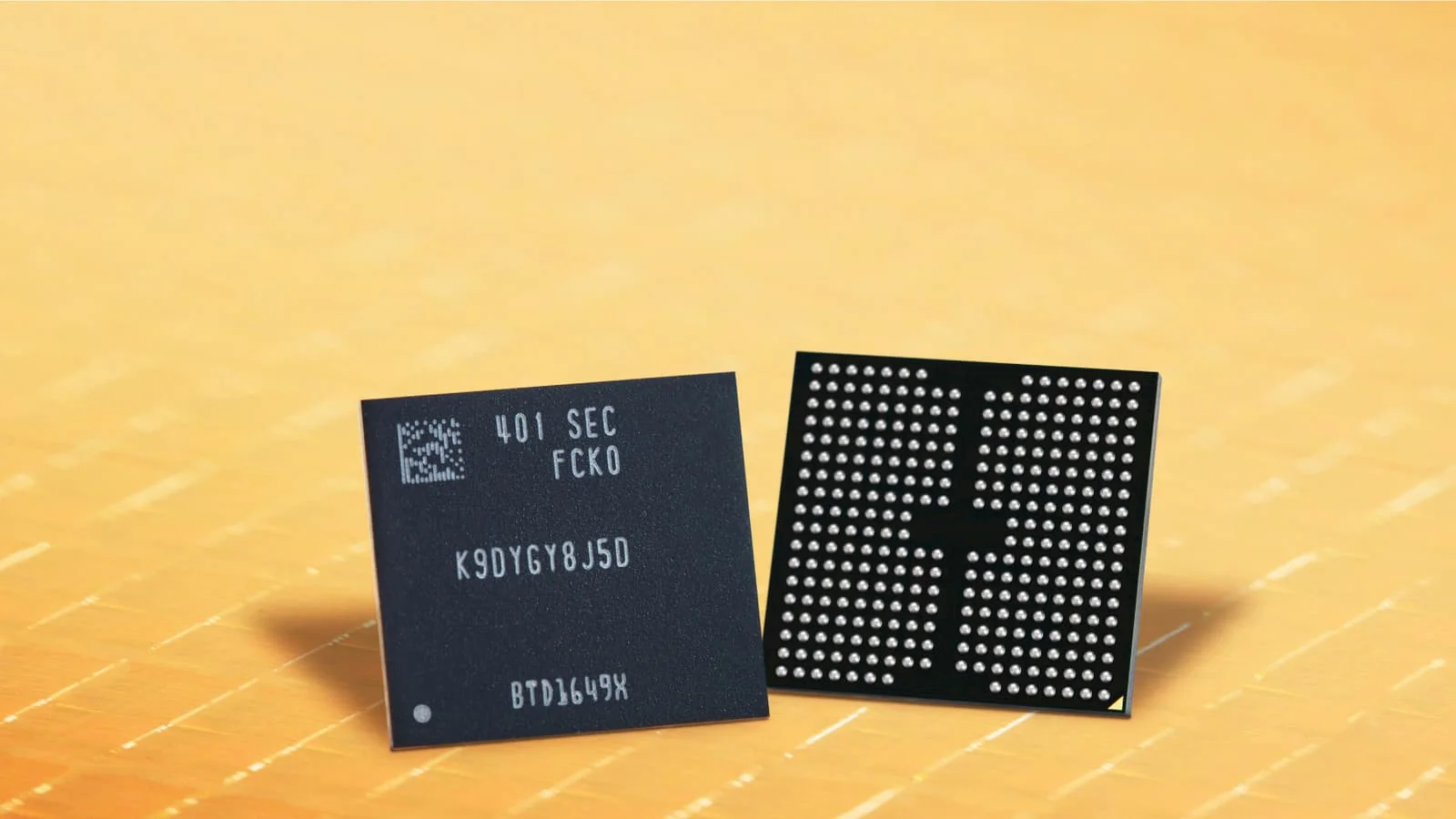
Samsung Electronics has developed the world's first 900-layer 3D NAND memory prototype. To achieve this, company engineers successfully combined two 450-layer crystals using CMB (Cell-on-Cell/multi-layer bonding) technology. This is reported by Ixbt.com reports .
According to Korean media, the functionality of the memory cells has already been verified in test samples. This technology involves bonding two separate NAND "skyscrapers" into a single 900-layer structure, which requires extreme precision and connection reliability.
During development, Samsung solved several technological challenges. Specifically, wafer deformation was eliminated, and errors were minimized thanks to a new method for correcting layer alignment.
Additionally, the bit line (BL) and word line (WL) architecture was improved. These changes allowed for reduced power consumption and optimized crystal dimensions. The creation of 900-layer NAND memory marks a new era in increasing data storage density.


Comments 0
…