


Intel Announces Manufacturing Technology for Massively Large Chips
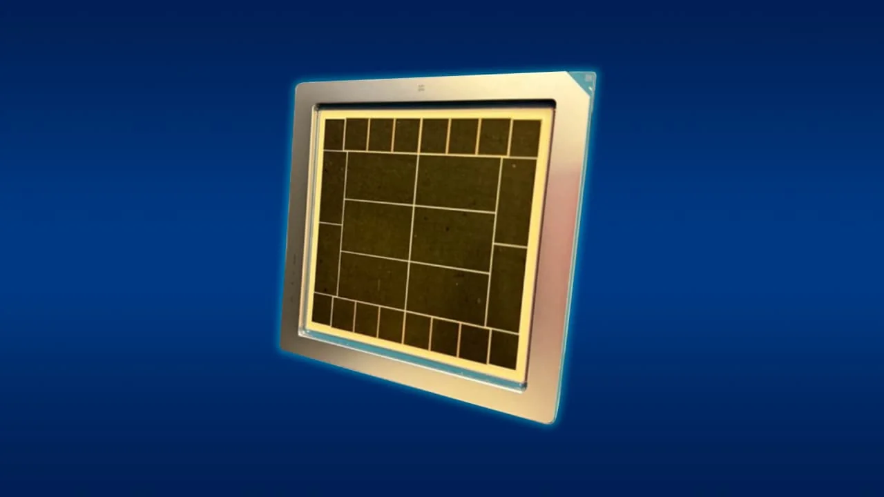
Intel announced that it has overcome significant technical barriers in semiconductor manufacturing and has gained the capability to create truly massive chips. According to ixbt.com, this is not about single monolithic crystals, but rather about modern chiplet solutions and advanced packaging technologies. This achievement will serve to sharply increase the efficiency of subsystems designed for AI infrastructure. This is reported by Ixbt.com reports .
At Intel's facilities in Rio Rancho, New Mexico, modern packaging technologies are significantly expanding the limited dimensions of photomasks. This will increase package sizes by eight times compared to current industry standards, and by more than twelve times by 2028. Experts compare this approach to a unique silicon mosaic, where specialized elements interconnect in a single massive package.
Unprecedented dimensions in the industry
Current modern packaging technologies make it possible to significantly exceed photomask dimensions and place more crystal microcircuits on a single substrate. However, certain physical limits existed until now, and Intel has successfully crossed one of them. The company emphasized that it has taken the next important step in developing extremely large form factor packages (HLFF).Extremely large packages created on the basis of the new technology will have dimensions of 240 x 240 millimeters. This will provide a 24-fold increase in photomask size and significantly outperform all indicators previously existing in the industry. Thus, Intel engineers are opening a completely new chapter in the microelectronics industry.
Ways to overcome technical difficulties
Implementing this massive project required solving a number of complex problems. In particular, the Intel Foundry team developed a gapless encapsulation process tested on packages with up to seven crystals. This directly eliminated one of the main manufacturing challenges that arose within the HLFF project.Experts also successfully resolved issues of warping that occur over such a large substrate area. For reference, due to difficulties such as physical strength and warping, other major market players, including NVIDIA, had abandoned the creation of the Rubin Ultra chip featuring two GPUs on a single substrate.
Such massive and complex structures are primarily necessary to meet the needs of the rapidly developing AI market. Intel's advanced technologies make it possible to directly place multiple computing chiplets and numerous memory chips on a single substrate, ensuring high performance.


Comments 0
…