


Huawei moves beyond Moore's Law: Details of the new LogicFolding 3D chips
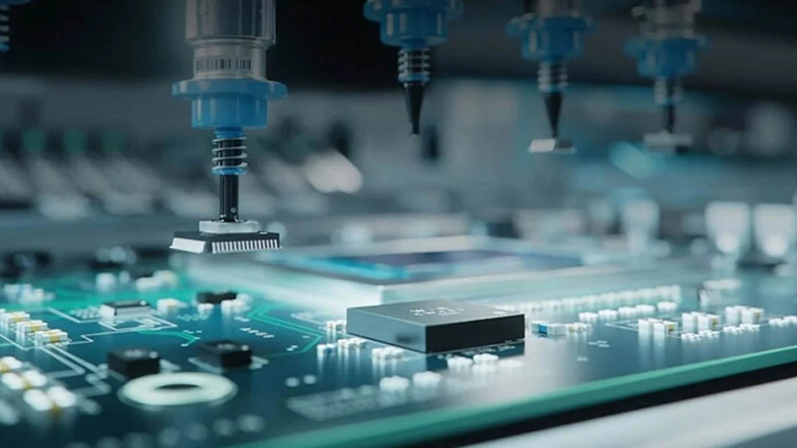
Researchers at Peking University have introduced 3D design tools based on Huawei's innovative microchip development: the LogicFolding architecture. Experts have developed an entirely new Electronic Design Automation (EDA) prototype to implement this method and apply the Tau scaling law. This is reported by Ixbt.com reports .
Although Huawei has been cut off from advanced international technologies, the company is focusing on creating its own independent solutions. The new EDA tool from Peking University views a multi-layer chip as a single structure during the design process. This allows for higher performance by optimizing all vertically stacked layers.
Tests conducted on an industry-grade open-source circuit showed that the new method reduces internal wire length by 30 percent. At the same time, the device's operating speed and heat dissipation properties are significantly improved compared to traditional methods. The system treats the entire SoC (System-on-Chip) as a single topology rather than viewing each layer separately.
He Tingbo, President of Huawei's semiconductor division, noted that Moore's Law will soon reach its physical limits. For this reason, the company considers the Tau law to be the new direction for the global microchip industry. It was also noted that no single company will be able to solve such complex problems alone in the coming decade.
The company plans to increase the power of its Kirin 5G processors this year using LogicFolding technology. New generation Kirin SoC chips based on this innovative technology are expected to hit the market in the fall of 2026.


Comments 0
…