


South Korea Develops Technology to Stack 10 Ultra-Thin Chips
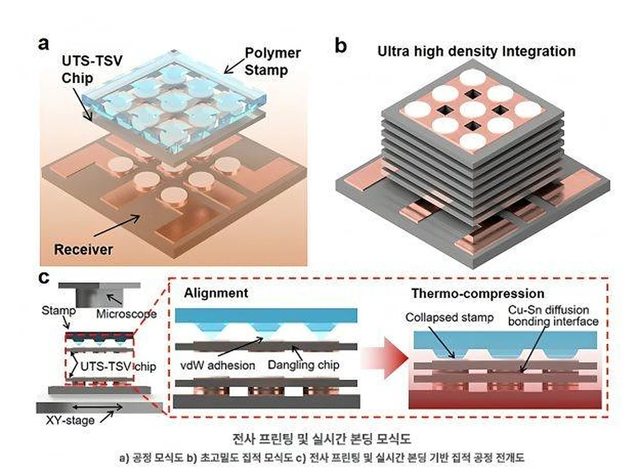
Scientists at the Pohang University of Science and Technology (POSTECH) in South Korea have announced a new assembly technology expected to revolutionize the semiconductor industry. This method allows for the stable stacking of over ten ultra-thin chips within a single package. This discovery will serve to drastically increase the power of modern gadgets and AI systems. This is reported by Ixbt.com reports .
The thickness of each layer created by the researchers is only 14 micrometers. For comparison, this is about five times thinner than a human hair. The new process combines two steps that were previously performed separately—precise placement of silicon crystals and the formation of inter-layer metal connections—into a single cycle. This significantly increases production efficiency.
New opportunities for HBM memory devices
Currently, in high-bandwidth HBM (High Bandwidth Memory) devices, multiple silicon layers are stacked vertically. However, as chips become ultra-thin, they become prone to bending and cracking. Increasing the number of layers makes it difficult to maintain precision during the assembly process. The method developed by POSTECH scientists is aimed at solving exactly this problem.The new technology allows for the creation of multi-layer structures at temperatures below 180 °C and pressures under 20 kPa. Due to these gentle conditions, chip deformation is minimized. During tests, even when more than ten layers were stacked, almost no misalignment was observed.
According to the researchers, the integration density achieved using this method is about 4 times higher than that of traditional 12-layer HBM memory. This means that significantly more computing elements can be placed in the same physical volume. This is especially important for AI accelerators from companies like NVIDIA, which require high performance and low power consumption in a limited space.
Application in future technologies
The new development can be widely used not only for memory chips but also in other areas of the semiconductor industry:- Chiplet packaging — combining several specialized integrated circuits into a single block;
- Manufacturing next-generation displays based on Micro LED technology;
- High-performance mobile processors and server systems.


Comments 0
…