IBM introduces the world's first sub-1nm chip technology
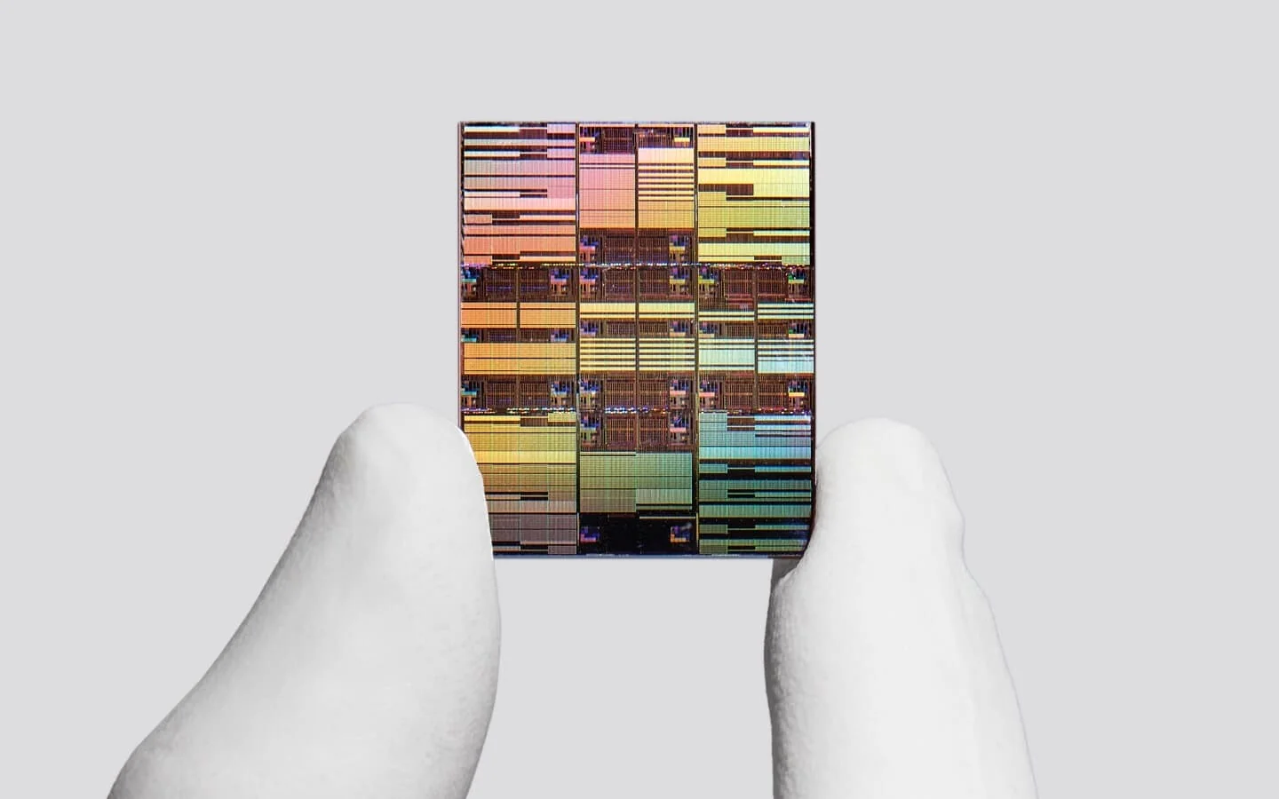
IBM, one of the leaders in the semiconductor industry, has taken a revolutionary step in the world of microelectronics. The company unveiled its new Nanostack architecture, which allows for nearly 100 billion transistors to be packed into a tiny crystal the size of a human fingernail. This development promises unprecedented power and energy efficiency for AI systems. This is reported by Ixbt.com reports .
The most sensational aspect of the new technology is that IBM calls it the world's first "sub-1nm" class chip. According to ixbt.com, the company has designated its platform as a "7 angstrom node". For reference, 1 angstrom is equal to one-tenth of a nanometer, meaning 7 angstroms is 0.7 nm. This figure represents a level of technological integration rather than the physical size of the elements.
Nanostack: Advantages of vertical stacking
According to modern laws of physics, transistors cannot be shrunk indefinitely due to problems such as quantum effects and current leakage. IBM engineers solved this obstacle by placing transistors not just side-by-side, but vertically on top of each other. The foundation of the Nanostack architecture relies on this vertical structure.Each base element consists of two vertically connected transistors, each containing three nanosheet layers with a thickness of only 5 nm. For comparison, this is equivalent to about 15 rows of silicon atoms. Such density allows for nearly doubling the number of elements compared to previous generation 2 nm technologies.
Energy efficiency and SRAM memory
According to IBM's estimates, transitioning to Nanostack technology can increase computing performance by 50 percent or reduce energy consumption by up to 70 percent. These metrics are vital for data centers and large AI models like ChatGPT, which consume massive amounts of electricity today.- 50 percent increase in computing power;
- 70 percent improvement in energy efficiency;
- 40 percent expansion in SRAM memory density.
Although this technology has so far only been demonstrated in laboratory conditions and at scientific symposiums, it is expected to serve as a foundation for future NVIDIA GPUs and Apple chips. Given that the 2 nm technology introduced by IBM in 2021 is currently being adopted as an industry standard, the era of 0.7 nm is not far off.


Comments 0
…