


Samsung allocates half of its 4 nm capacity to HBM4 base dies
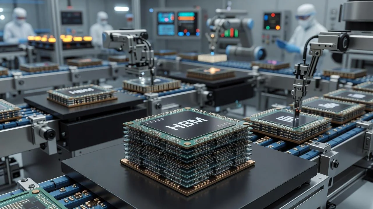
South Korean tech giant Samsung has redirected a significant portion of its 4 nm process capacity toward memory production. According to ZDNet, more than half—specifically 50-60%—of these advanced capacities have been allocated to producing base dies for next-generation HBM4 memory. This strategic move is driven by the surging demand for components designed for AI and high-performance computing systems. This is reported by Ixbt.com reports .
It is known that Samsung is one of the leaders in supplying chips based on 2 nm standards. However, such SoCs remain limited, and the company's primary semiconductor products are still manufactured using 4 nm technology. Currently, a large portion of these capacities has been adapted for the infrastructure required to create modern memory modules.
HBM4 architecture and base dies
HBM (High Bandwidth Memory) consists of a special stack of multiple DRAM chips. At the foundation of this complex structure lies the base die. Although the memory itself is created using entirely different methods and technological processes, the base die serving as its foundation is manufactured on lines typically used for logic SoC chips.This is precisely why Samsung has mobilized more than half of its total capacity from the previous generation 4 nm process for this task. According to the source, the total capacity of the relevant production lines is 30,000 silicon wafers per month. This allows the company to stably meet the demand for the latest types of memory modules.
Experts believe that the rapid development of AI technologies and the expansion of data centers are further strengthening the integration between memory and processors. Samsung's allocation of 4 nm lines for HBM4 base dies is linked to the need for rapid adaptation to market demands. Consequently, the company aims to further solidify its position in the high-speed memory segment.


Comments 0
…