


Scientists learn to create OLED screens using photolithography like microchips
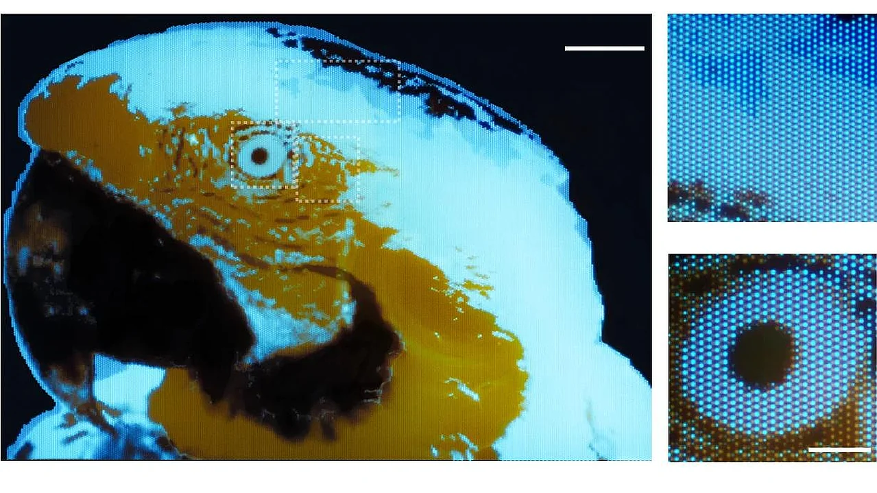
Scientists at ETH Zurich have developed a new type of organic light-emitting material compatible with photolithography, a technology widely used in modern microchip manufacturing. According to Ixbt.com, this discovery could significantly simplify the process of creating ultra-small, high-resolution OLED displays for future augmented reality glasses, camera viewfinders, sensors, and medical equipment. This was reported by Ixbt.com reports.
OLED technology is well-suited for miniaturization because its organic materials maintain high brightness even in very small light-emitting elements. However, manufacturing microscopic pixel elements with high precision remains a complex task. The standard photolithography method is not well-suited for this purpose because the solvents and other chemicals used in the process can damage delicate organic components.
New material and its operating principle
To solve this problem, ETH Zurich researchers proposed a material that functions simultaneously as a photoresist and a light-emitting element, capable of withstanding the chemical processes of photolithography. This material has a "core-shell" structure, with a light-emitting molecule protected from external influences in the core and reactive groups on the surface.After exposure to ultraviolet radiation, these groups form cross-links, and the irradiated areas become insoluble. As a result, it becomes possible to form microscopic structures from the light-emitting material, similar to the method used in semiconductor manufacturing.
Experimental results and prospects
Scientists demonstrated the capabilities of their technology using a multi-colored fluorescent parrot image measuring just 300 × 430 μm. It consists of 250 × 350 pixels, or 87,500 individual dots. The researchers note that this image has the highest resolution among multi-colored fluorescent images created using photolithography.Nevertheless, this sample is not yet a full-fledged display because its pixels do not form an image on their own when an electrical signal is applied, but rather glow under external light. At the same time, experts demonstrated that the developed material can also work in electroluminescence mode. For this, they created an ETH light-emitting logo measuring 1 × 2.4 mm based on organic light-emitting diodes.
To implement the technology in full-fledged displays, the next step requires further miniaturization of light elements and the creation of electronics capable of independently controlling individual microscopic pixels. Only when these tasks are solved will it be possible to apply it in practice.
It is noted that the scope of this development is not limited to screens. Controllable microscopic light sources can be placed directly on the chip itself for biological and medical research, microscopy, and sensors. For example, such elements can be used to illuminate individual cells or to influence nerve cells using light.


Comments 0
…